
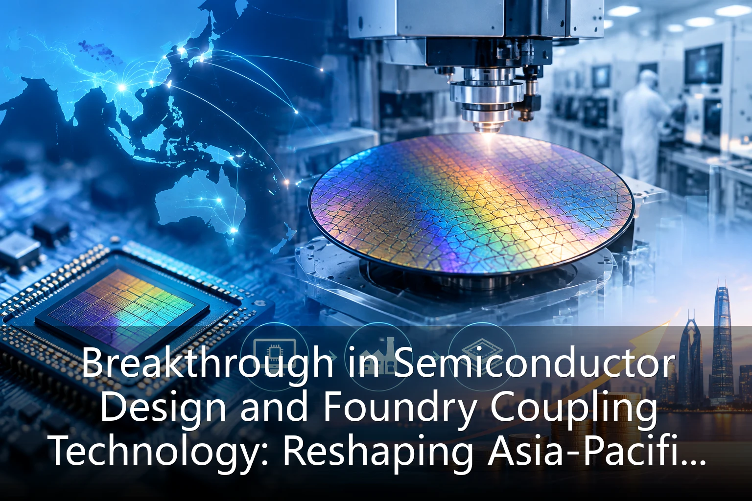
Breakthrough in Semiconductor Foundry‑Coupling Technology: Reshaping the New Landscape of Global Semiconductor Manufacturing
As the global semiconductor industry enters a period of profound adjustment, technological innovation has become the core driving force for industrial development. Since 2026, major breakthroughs have been achieved in semiconductor foundry‑coupling technology. This innovative model integrating chip design and manufacturing links is reshaping the global semiconductor industrial chain and bringing unprecedented opportunities and challenges to the sector. As part of OceanRing Asia‑Pacific Finance’s Global Semiconductor Trade Insight Column, this article provides an in‑depth analysis of the latest developments in semiconductor foundry‑coupling technology, examines its impacts on the global semiconductor‑trade landscape, and delivers forward‑looking market insights for investors.
Rise and Evolution of Semiconductor Foundry‑Coupling Technology
Semiconductor foundry‑coupling technology, also referred to as “design‑manufacturing integration technology”, leverages advanced algorithms and manufacturing processes to achieve high‑level consolidation of chip design and fabrication, enabling seamless hand‑offs from design through to manufacturing. This technological breakthrough arises from the dual‑headwinds confronting the semiconductor industry: the slowing of Moore’s Law and escalating costs for advanced process nodes. It represents a vital pathway for the industry to pursue innovative advancement.
According to the Q2 2026 Global Chip Trade Analysis Report released by OceanRing Asia‑Pacific Finance, the market size for semiconductor foundry‑coupling technology is projected to expand from USD 28 billion in 2025 to USD 42 billion in 2026, registering an annual growth rate of 50%. Such rapid expansion demonstrates the market’s urgent appetite for technological innovation as well as strong investor confidence in this field.
The core strengths of semiconductor foundry‑coupling technology are as follows:
- Lower barriers to design: Standardized interfaces and toolchains allow small‑to‑midsize design‑houses to access advanced manufacturing processes.
- Improved production yield: Real‑time feedback loops during fabrication deliver substantial improvements in chip yield rates.
- Shortened R&D cycles: Concurrent progression of design and manufacturing drastically cuts time‑to‑market for new products.
- Reduced costs: Fewer iterative trial‑and‑run cycles, optimized resource deployment and lower overall R&D expenditure.
Global Development Landscape for Semiconductor Foundry‑Coupling Technology
Currently, the global landscape for semiconductor foundry‑coupling technology features a “tripartite” development pattern. The United States, Asia and Europe each emphasize distinct priorities, creating a differentiated competitive environment.
The United States: Leader in Technological Innovation
U.S.‑based enterprises occupy a globally leading position in R&D for semiconductor foundry‑coupling technology. Leading chip designers such as NVIDIA and AMD have built deep‑seated collaborative relationships with foundry giants TSMC and Samsung to jointly advance the innovation and deployment of foundry‑coupling technology.
During the first half of 2026, NVIDIA and TSMC announced a joint project to develop AI chips built upon the 2 nm process node. Adopting state‑of‑the‑art foundry‑coupling technology, the initiative tightly merges design optimisation with fabrication workflows to substantially boost chip performance and energy efficiency. This collaboration marks a key commercial milestone for foundry‑coupling technology and is expected to steer the direction of industry‑wide technological evolution.
Asia: Pioneer in Industrial‑Scale Deployment
Across Asia, notably mainland China, Chinese Taiwan, South Korea and Japan, remarkable progress has been made in the industrial roll‑out of semiconductor foundry‑coupling technology. These geographies host complete semiconductor industrial ecosystems, forming a solid foundation for rapid commercial adoption.
Semiconductor design firms in mainland China, including HiSilicon and Unisoc, are actively embracing foundry‑coupling technology to accelerate R&D for high‑end chips. Meanwhile, foundries such as SMIC and Hua Hong Semiconductor keep elevating their process capabilities to furnish design houses with more sophisticated manufacturing support.
TSMC in Chinese Taiwan regards foundry‑coupling technology as a core competitive advantage. Leveraging advanced packaging solutions including CoWoS (Chip on Wafer on Substrate), the firm realises deep coordination between design and manufacturing and consolidates its leading standing within the global semiconductor foundry sector.
Europe: A Differentiated Development Path
Europe pursues a differentiated strategy for semiconductor foundry‑coupling technology, concentrating on targeted verticals such as automotive electronics and industrial controls. European enterprises including Infineon and STMicroelectronics cooperate with local foundries to develop application‑specific foundry‑coupling solutions.
In 2026, the European Union activated the European Chips Act and scaled up support for R&D into semiconductor foundry‑coupling technology, with the objective of strengthening Europe’s position within the global semiconductor value chain. This policy orientation delivers robust governmental backing for the advancement of European foundry‑coupling capabilities.
Impacts of Semiconductor Foundry‑Coupling Technology on the Global Trade Landscape
Breakthroughs in semiconductor foundry‑coupling technology are exerting profound effects on global semiconductor trade, primarily reflected in the following dimensions:
Restructuring of Industrial Chains
Within the traditional semiconductor ecosystem, design houses and fabrication facilities operated relatively independently. The advent of foundry‑coupling technology is driving the industrial chain toward a “design‑manufacturing integrated” paradigm. This transformation is reshaping the geographic layout of the global semiconductor industry and fostering new industrial clusters.
Benefiting from a full‑fledged industrial chain and sizable market demand, the Asia‑Pacific region is emerging as the global hub for the industrialisation of foundry‑coupling technology. According to monitoring data from OceanRing Asia‑Pacific Finance, investments tied to semiconductor foundry‑coupling technology within Asia‑Pacific accounted for 62 % of total global investment in H1 2026, representing a 15‑percentage‑point increase year‑on‑year versus 2025.
Shifts in Trade Flows
Broad‑based adoption of foundry‑coupling technology is reshaping global semiconductor trade flows. On one hand, deepening technical cooperation between design and manufacturing participants fuels growth in high‑end technology‑oriented trade. On the other hand, as foundry‑coupling technology matures and standardisation improves, trade volumes for certain intermediate components gradually decline.
During H1 2026, the trade value of precision casting components for semiconductor equipment climbed 35 % year‑on‑year, demonstrating upstream equipment demand stimulated by foundry‑coupling technology. Concurrently, trade in high‑end chip‑design services expanded rapidly at an annual growth rate of 45 %, signalling rising demand for specialised services under the integrated design‑manufacturing operating model.
Deepening Regional Collaboration
Advances in semiconductor foundry‑coupling technology have facilitated deeper integration of regional semiconductor industrial chains. In 2026, the European Union and South Korea concluded a semiconductor supply‑chain cooperation agreement and set up a joint R&D centre for foundry‑coupling technology. The Association of Southeast Asian Nations also announced the launch of a regional development programme targeting semiconductor foundry‑coupling technology, aimed at lifting regional industrial competitiveness.
These regional collaborative initiatives are remoulding global semiconductor‑trade dynamics, fostering a region‑oriented development model anchored on technological cooperation and exerting far‑reaching repercussions on the established global semiconductor trading system.
Investment Opportunities and Associated Risks
Breakthroughs in semiconductor foundry‑coupling technology unlock abundant investment prospects for global investors while also bringing inherent risks. The analyst team at OceanRing Asia‑Pacific Finance identifies the following areas worthy of investor attention:
Core Equipment and Materials
The industrialisation of foundry‑coupling technology imposes new requirements for high‑end semiconductor equipment and materials, and relevant manufacturers stand to capture excess returns. Market analysis forecasts that the market for foundry‑coupling‑related semiconductor equipment will reach USD 38 billion over 2026‑2027, sustaining annual growth above 35 %. The high‑end materials segment is also set for rapid expansion.
Investors may focus on enterprises holding core competitive strengths in advanced lithography systems, precision metrology instruments and high‑purity materials; such players are well‑positioned to capitalise on the foundry‑coupling technology trend.
Collaborative Design‑Manufacturing Platforms
Growing adoption of semiconductor foundry‑coupling technology creates development opportunities for platform‑type companies delivering integrated design‑manufacturing collaboration services. These firms supply standardised interfaces, toolkits and professional services to enable efficient coordination between design houses and foundries and lower technical entry barriers.
Global financing raised for semiconductor design‑manufacturing collaboration platforms hit USD 6.5 billion in H1 2026, rising 58 % year‑on‑year, which underscores robust capital‑market enthusiasm for this segment. Investors may prioritise platform enterprises distinguished by proprietary core‑technology assets and extensive domain expertise.
Specialised Services and Talent
Deployment of foundry‑coupling technology raises the bar for professional talent, which will in turn fuel rapid growth for associated training, consulting and talent‑service markets. Meanwhile, cross‑disciplinary professionals with mixed technical backgrounds will become scarce industry resources; corporate talent strategies will directly determine market competitiveness.
Risk Factors
Notwithstanding bright long‑term prospects for semiconductor foundry‑coupling technology, investors ought to keep the following risk factors in view:
- Risk of rapid technological iteration: Fast‑paced semiconductor innovation creates the threat that foundry‑coupling technology may eventually be superseded by newer technologies.
- Geopolitical risks: The global semiconductor industrial chain remains highly exposed to geopolitical turbulence; trade restrictions and technology blockades could impede technical progress.
- Risk of investment overheating: The field currently enjoys strong investment momentum, raising the possibility of short‑term market bubbles.
- Talent shortage risk: Extended lead‑times required to nurture cross‑disciplinary specialists risk creating a bottleneck constraining industrial expansion.
Future Outlook
Looking ahead, semiconductor foundry‑coupling technology will continue to evolve in depth, with the following trends taking shape:
Accelerated Technological Convergence
Semiconductor foundry‑coupling technology will undergo deep fusion with cutting‑edge disciplines including artificial intelligence and quantum computing, giving rise to smarter collaborative design‑manufacturing ecosystems. By 2028, AI‑driven foundry‑coupling technology is expected to become the mainstream industry standard, supporting advanced autonomous optimisation and decision‑making workflows.
Expanding Application Horizons
Use‑cases for foundry‑coupling technology will stretch beyond high‑performance computing chips into automotive electronics, industrial control, the Internet of Things and further vertical sectors. Within automotive electronics specifically, surging demand for high‑performance chips driven by rapid advances in autonomous driving will unlock broad application scope for foundry‑coupling solutions.
Co‑existence of Globalisation and Regionalisation
On one hand, rising standardisation of foundry‑coupling technology will bolster globalised industry development. On the other hand, deepening integration within regional industrial chains will reinforce regionalised trajectories, yielding a landscape in which globalisation and regionalisation develop side‑by‑side.
Sustainable Development as a Key Consideration
Mounting global emphasis on sustainability will push semiconductor foundry‑coupling technology toward greener manufacturing practices and improved energy efficiency to lessen environmental footprints. In coming years, ESG considerations are projected to constitute a vital evaluation metric for foundry‑coupling technology, influencing corporate capital allocation decisions and market performance.
Conclusion
Breakthroughs within semiconductor foundry‑coupling technology are reshaping the global semiconductor manufacturing landscape and opening unprecedented developmental opportunities for the industry. As part of OceanRing Asia‑Pacific Finance’s Global Semiconductor Trade Insight Column, we continue tracking real‑time developments across this sector and deliver timely, professional market analysis as well as investment guidance for investors.
Against the backdrop of sweeping adjustments across the global semiconductor sector, semiconductor foundry‑coupling technology is poised to emerge as a pivotal growth engine for the industry. Investors should closely monitor technological trajectories, seize investment opportunities created by industrial‑chain restructuring, rationally evaluate underlying risks, and make well‑informed investment decisions.
With continuous technological refinement and expanding practical deployments, semiconductor foundry‑coupling technology will assume an increasingly critical role within global semiconductor trade, remaking industrial value chains and generating fresh growth drivers. OceanRing Asia‑Pacific Finance will sustain ongoing coverage of developments in this field, furnishing investors with in‑depth market insights and specialised investment guidance.
Disclaimer: This translation is for reference only and does not constitute investment advice.